What the Free Flying-Probe Test on Your Bare PCB Actually Catches
Every bare PCB we supply is 100% flying-probe tested for opens and shorts. Here is what that test finds, what it cannot find, and how your files make it better.
Microplacer team · 15 November 2026 · 5 min read
 Quality & Testing
Your boards arrive, you solder the first one, and it does not boot. Is it the PCB, the parts, the soldering or the design? Knowing what the free flying-probe test has already ruled out on every bare board saves you hours of guessing — and knowing what it cannot rule out tells you where to look next.
Bare board testing and assembled board testing are different jobs
People often hear “tested” and assume the whole circuit has been checked. In practice there are two separate stages. A bare board test happens before any components are fitted and asks one question: is the copper connected exactly as the design data says? An assembled board test happens after soldering and asks about joints, part values, orientation and, with a functional test, whether the product actually works.
| Bare PCB electrical test | Assembled board (PCBA) test | |
|---|---|---|
| When | After fabrication, before assembly | After components are soldered |
| Compared against | The connections defined by your design files | Your schematic, BOM and test plan |
| Looks for | Opens and shorts in the copper | Solder faults, wrong or missing parts, circuit behaviour |
The free test we run on every bare PCB is the first kind. It makes sure you start assembly on boards whose copper is right, so you do not spend components and soldering time on a board that was never going to work.
How a flying probe checks your board
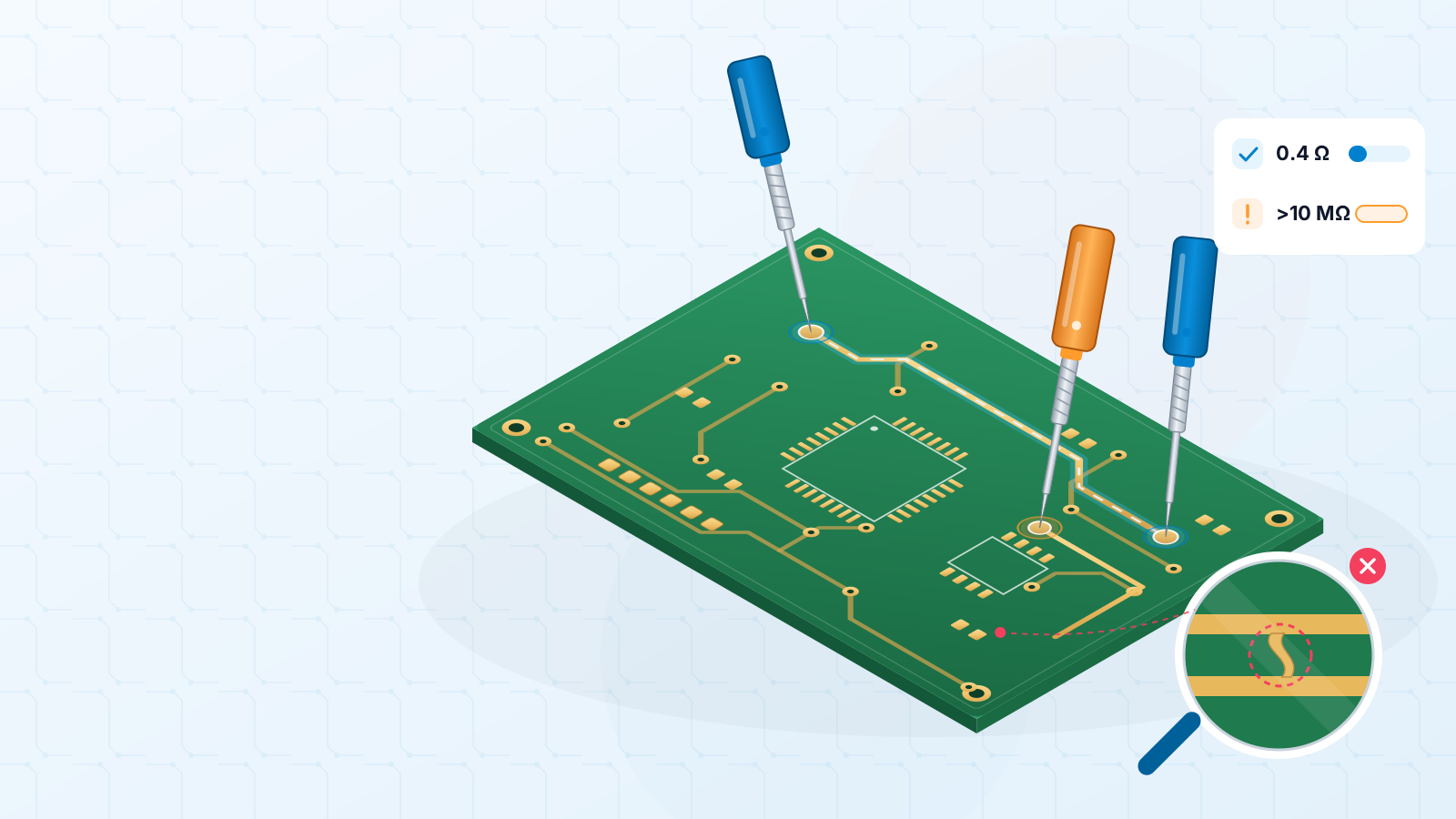
A flying-probe tester uses a few motorised probes that move across the board and touch pads, vias and test points one after another. There is no custom fixture, which is why it suits prototypes and small batches where the design may still change. The test program is built from your design data, and it runs two kinds of checks:
- 1Continuity — every point on a net should be connected to every other point on that same net. The probe measures between the ends of each net and expects a low resistance.
- 2Isolation — every net should be separated from its neighbours. The probe measures between nets that should not touch and expects a very high resistance.
A board passes only when every net is both continuous and isolated. Acceptance limits for this kind of test are described in IPC-9252, the IPC standard for electrical testing of unpopulated boards.
What it finds
- Opens — a track etched through, a nick that broke a thin trace, or a connection that never formed between layers.
- Shorts — a copper sliver left between two tracks, a bridge between close pads, or an inner-layer short you could never see from the outside.
- Plating problems in vias and holes — a via with a void in its barrel can break the path between layers. On multilayer boards this is exactly the kind of fault that is invisible without an electrical test. (A barrel that is thin but still conducting will usually pass; plating thickness is checked by other means, such as cross-sections.)
All of these are fabrication defects: the board does not match your design. Catching them on the bare board is far cheaper than finding them later under a BGA or inside a finished enclosure.
What it does not find
The test compares the board with your data, not with your intentions. That gives it some clear limits:
| Problem | Caught by bare-board test? | Where it is caught instead |
|---|---|---|
| A trace missing in your layout | No — the board matches your data | Design review and DRC before ordering |
| Wrong footprint or swapped pins | No | Schematic and footprint checks, first-article bring-up |
| Faulty or wrong-value component | No — no parts are fitted yet | Electrical test or functional test after assembly |
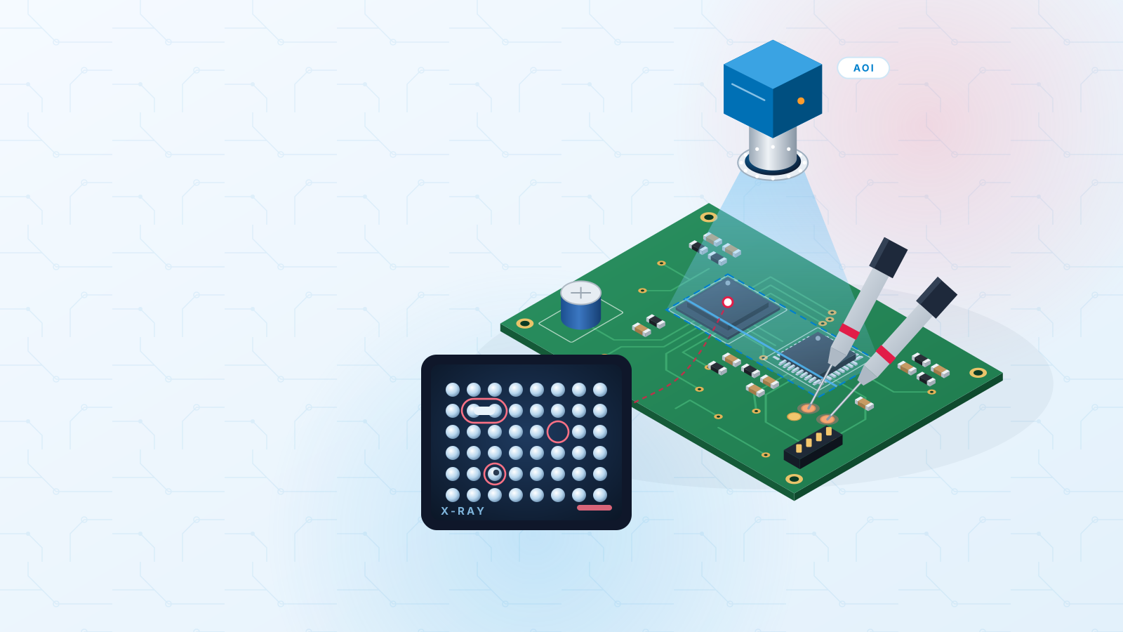
| Solder bridge or open joint | No | Visual inspection, AOI, X-ray, electrical test of the PCBA |
| Firmware or circuit behaviour | No | Functional test with your test plan |
So a board that passed the flying probe and still does not work is pointing you towards the design, the components or the assembly — not the bare copper. Our PCBA testing and inspection guide explains the methods used at that stage.
Why every board is tested, free
Sampling a few boards from a batch would miss the one board with a hidden inner-layer short — and that is the board that ends up on your bench at midnight. That is why 100% of bare PCBs we supply go through the flying-probe electrical test, and it is included in the price rather than offered as an add-on. If your project needs anything beyond opens-and-shorts testing, write it in your production notes so our engineers can compare it with our options.
How good design data helps the test
The test is only as good as the data it is built from. A few habits make it more useful:
- 1Send a complete, consistent file set — all copper layers, drill files and the board outline from the same revision.
- 2Include an IPC-D-356 netlist if your CAD tool can export one; it gives an independent reference to compare the Gerbers against.
- 3Avoid leftover copper or test text on copper layers that is not meant to be there — it becomes part of the board.
- 4Write any special requirements as production notes in your files; our engineers read them and compare them with our options.
Next step
Have questions about testing, quality or what happens to your files? The PCB manufacturing FAQ covers testing and orders, and our quality standards page explains how we approach quality across production.
#flying-probe#electrical-test#bare-board-test#pcb-quality#opens-and-shorts
Get an instant PCB quote