Through, Blind, Buried, Tented, Plugged: Vias Explained Without the Jargon
A plain-language tour of via types and covering options — through, blind, buried, microvia, tented, plugged, filled — and how to pick the simplest one your board actually needs.
Microplacer team · 15 November 2026 · 4 min read
 PCB Design
Open the high-spec section of any PCB calculator and you meet a wall of words: blind, buried, tented, plugged, filled and capped. It is easy to tick something that sounds advanced and pay for it without needing it. Here is what each term really means, and which one your board most likely needs (spoiler: usually the cheapest).
What a via does and why its type affects cost
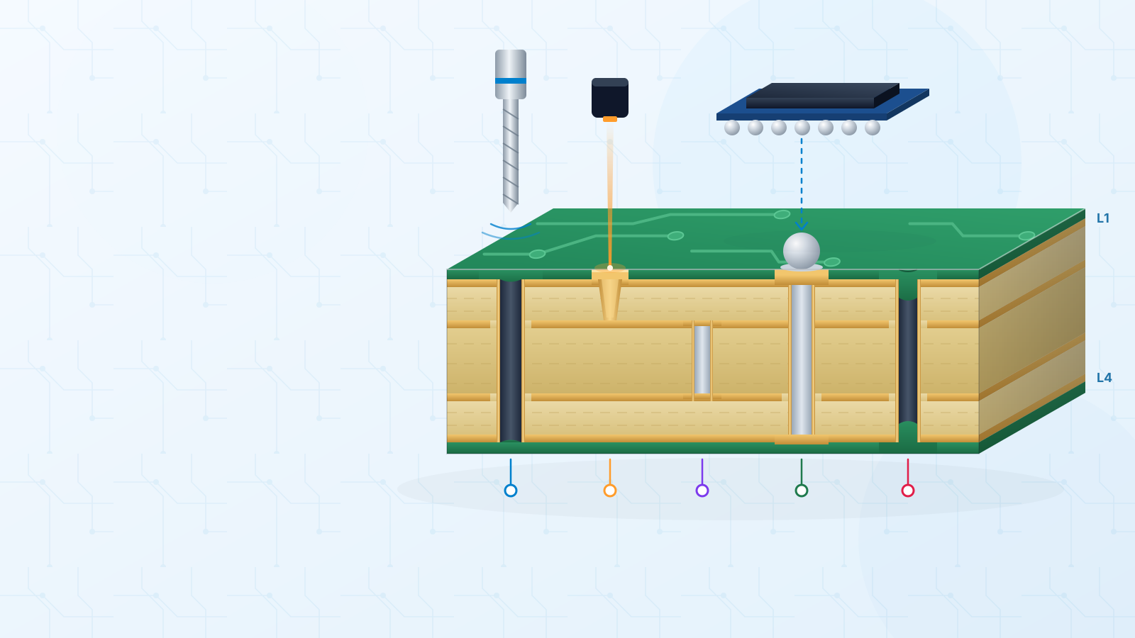
A via is simply a small plated hole that carries a signal or power from one copper layer to another. The hole is drilled, the walls are coated with copper, and the trace on one layer now continues on another. That is all a via does electrically.
Cost comes from how the hole is made and finished. A hole drilled once through the finished board is the easy case. A hole that must stop part-way, live only between inner layers, or be filled and plated flat needs extra drilling, lamination or plating steps — and every extra step adds time, cost and a little yield risk.
Through-hole vias: the default for most boards
A through-hole via goes from the top layer all the way to the bottom. It is drilled after the layers are pressed together, so one drilling and plating pass handles every via on the board. That is why it is the standard choice on almost every 2- to 16-layer design, and the only via type included in our instant online price.
The one number worth watching is the aspect ratio: board thickness divided by drill size. Put a 0.25 mm drill in a 1.6 mm board and you get about 6.4:1. As that ratio climbs, plating solution struggles to reach the middle of a long, narrow hole, so the copper in the barrel can end up thin. If you are pushing very small vias, a thinner board or a slightly larger drill gives you margin.
Blind, buried and microvias: when HDI is worth it
| Via type | Where it goes | Why you would use it |
|---|---|---|
| Blind via | From an outer layer to an inner layer; visible on one side only. | Frees routing space on the other side under dense parts. |
| Buried via | Between inner layers only; invisible from outside. | Adds connections when the outer layers are already full. |
| Microvia | Tiny laser-drilled hole, usually spanning one thin dielectric layer. | Escaping fine-pitch BGAs, often placed directly in the pad. |
These are the building blocks of HDI (high-density interconnect) boards. Instead of pressing all layers once, the board is built in stages — each stage adds lamination, drilling and plating — so price and production time follow how many sequential pressings the design needs, not just how many copper layers it has.
As general guidance, you are probably in HDI territory if:
- You have BGAs or CSPs at 0.5 mm pitch or finer.
- A large BGA cannot be fanned out with a via beside each pad (the “dog-bone” pattern).
- The outline is fixed and small, and the layer count keeps climbing with through vias alone.
If your parts are 0.8 mm pitch or coarser and there is room to fan out, a normal multilayer board is usually cheaper and quicker. Blind, buried and microvia designs are not priced instantly — send your files and our team reviews the stack-up and quotes it.
Tented, plugged, filled and via-in-pad: covering options compared
Separate from via type is via covering: what happens to the hole opening on the surface. This matters most if the board will be assembled.
| Covering | In plain words | Pick it when |
|---|---|---|
| Tented | Solder mask covers the via pad and opening. | Almost always. It is the standard, no-extra-cost default. |
| Untented | Via pad and hole left open. | You want to probe or solder to the via; keep it away from SMD pads. |
| Plugged | Hole sealed with mask ink or plugging material, surface not plated flat. | Vias near fine-pitch parts, to stop solder and flux passing through. |
| Epoxy filled & capped | Hole fully filled with resin, sanded flat, copper plated over. | Via-in-pad under BGA and QFN pads. |
| Copper paste filled & capped | Filled with conductive paste, flattened and plated over. | Via-in-pad where extra heat or current flow helps. |
Why via-in-pad needs filling
An open hole in a solder pad behaves like a drinking straw. During reflow, molten solder is pulled into it, leaving a starved joint, voids under a thermal pad, or solder balls on the far side. Filling and capping the via (IPC-4761 describes this type) turns it back into a flat, solid pad. Plugged is not the same thing — the surface is not made flat, so do not put a plugged via directly inside an SMD pad.
Ordering assembly with BGA, LGA or 0201 parts? Those designs go to an engineering review before they are priced, which is a good moment to confirm that every via sitting in a pad is filled and capped.
Special holes: castellated, countersunk, slots and plated edges
- Castellated holes — plated half-holes along the edge so a module can be soldered onto another board. Draw the full pad and hole across the outline so half remains after routing.
- Countersunk holes — a cone at the top of the hole so a flat-head screw sits flush. Mark which holes you mean.
- Slots — oval or long holes, plated or not, for flat-pin parts such as DC jacks and USB shells. Draw them as slots in the drill file or on a mechanical layer.
- Plated edges — copper along the board's side walls tied to ground, used for shielding and grounding to a metal enclosure.
For any special hole, a short note or drawing listing positions and sizes saves a round of questions — production notes in your uploaded files are read and compared with the options you selected.
Rule of thumb: pick the simplest via that meets the design
- 1Start with tented through-hole vias. They suit the large majority of boards and cost nothing extra.
- 2Use the largest via size your routing allows, and keep the aspect ratio modest.
- 3Add plugging only where vias sit close to fine-pitch pads.
- 4Use filled and capped vias only for via-in-pad under BGAs, QFNs or similar.
- 5Move to blind, buried or microvias only when fine pitch or a fixed outline truly leaves no other route.
Ready to go deeper? Our vias and special holes guide covers every calculator option in detail, the HDI design guide explains build-ups and microvia stacks, and PCB capabilities shows what can be priced instantly online.
#vias#via-in-pad#hdi#pcb-design#special-holes
Get an instant PCB quote