9 DFM Mistakes That Hold Up Your First PCB Order
Most engineering queries on a first PCB order come from a few avoidable design and file mistakes. Here are nine of them and a quick checklist to catch them before upload.
Microplacer team · 15 November 2026 · 5 min read
 PCB Design
You have finished the layout, the DRC is green and the Gerber zip is ready. Then, a day after you order, an email arrives: our engineers have a question about your files. For a first board this is very common, and almost always it comes from a short list of avoidable mistakes. Here are nine of them, and how to catch each one before you press upload.
Why files are checked, and what a query costs you
An engineer opens every order before production starts. They hold your Gerber up against the options you chose (layers, size, thickness), make sure the tracks, gaps and holes are within what can be built, and look for things that seem unintended, like a reference designator printed across a pad. When something needs attention, you hear from us before anything is made.
That saves you from a bad batch, but your order waits while the question is open. A CAD fix plus a fresh export can easily eat a day or two of the 10–15 working days you planned around, so the best query is the one never sent.
Mistake 1: Trusting design rules you never set
A green DRC only proves the layout obeys the rule set inside your CAD tool. If that rule set allows 0.1 mm tracks, nothing will warn you when the board is full of them. Copy your track, gap, via and clearance limits from our PCB capabilities table into the tool on day one, so every trace you draw is already buildable.
Mistake 2: Tracks and gaps pushed to the limit everywhere
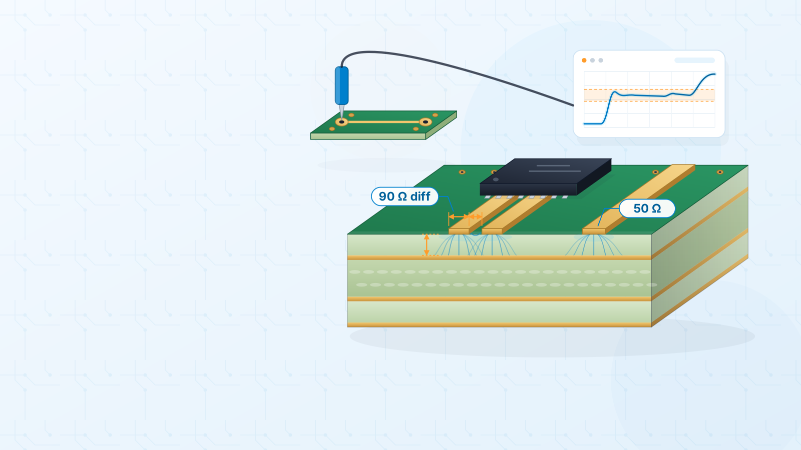
Fine tracks are possible, but each step toward the limit makes etching less forgiving. Beginners often route the whole board at the minimum because one fine-pitch IC needed it. Instead, run signal tracks at around 0.2 mm (8 mil) or wider where there is room, keep gaps at least as wide as the track, and neck down only near the tight part. For power tracks, size them with an IPC-2152 based calculator and remember that heavier copper needs wider gaps.
Mistake 3: An annular ring that is too thin
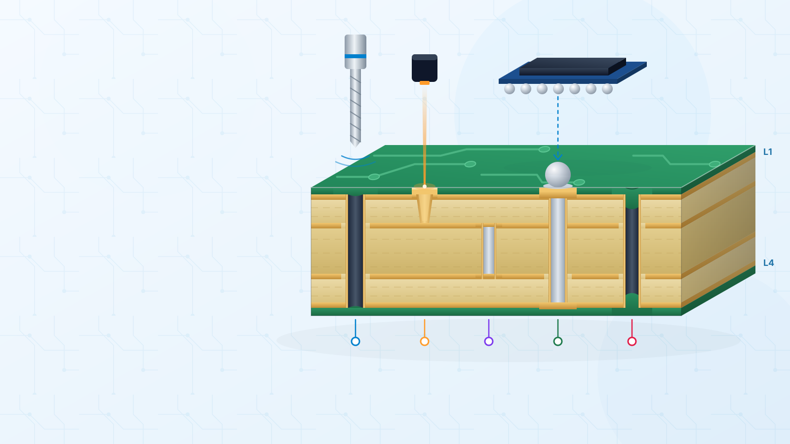
The annular ring is the copper left around a hole after drilling: (pad diameter − hole diameter) ÷ 2. Drills are never perfectly centred, so a thin ring can break out and cut the connection. As general guidance, aim for roughly 0.15 mm or more on vias and more on pads you will solder. Also remember the drill for a plated hole is slightly larger than the finished hole, so check the datasheet hole size for through-hole leads.
Mistake 4: Copper hugging the board edge and holes
The router bit and the V-cut blade both take away material along the outline, and any copper in their path gets nicked, smeared or left bare. Pull pours and traces back from milled edges, and give V-score lines an even wider margin, because the blade cuts a groove into both faces. Treat non-plated mounting holes the same way: a screw head or washer resting on the board can bridge to copper that sits too close. If you genuinely need metal on the board edge, ask for edge plating as an option instead of drawing copper up to the line.
Mistake 5: Silkscreen on pads
Legend ink on a pad stops solder from wetting it. Reference designators dropped on top of footprints, logos dragged across a connector, and part outlines drawn over pad edges are the usual culprits. Most CAD tools can clip the silkscreen to the mask openings; switch that on. Keep text at about 1 mm high with a line width near 0.15 mm or more, or it may print blurred.
Mistake 6: No polarity or pin-1 marks
A diode, electrolytic capacitor or IC with no clear marking turns assembly into guesswork. Put the cathode bar, the + sign and the pin-1 dot beside the part, not underneath it, so they are still visible once the part is fitted. If you plan to order assembly, make sure the silkscreen designators match your BOM and pick-and-place file.
Mistake 7: A missing or ambiguous board outline
The outline tells the router where to cut. Problems we see often: tiny gaps at arc joins, overlapping segments, an outline on two different layers, or a slot drawn only on silkscreen. Draw one closed shape on a single outline layer, and put cut-outs and slots on that same layer.
Mistake 8: Production notes hidden in the files
Some designers write "ENIG, 2 oz, black mask" in a text layer and choose different options in the order form. We do read production notes in your uploaded files and compare them with the options you selected, but a conflict means a query. The simple fix: select what you want in the calculator so the price matches the board, and use notes only for things the form cannot express.
Mistake 9: A layer count or via size that does not match the order
A 4-layer Gerber ordered as a 2-layer board, or a drill file with vias smaller than the min via option you picked, will always be stopped. Count the copper layers in your zip, and on boards with four or more layers look up the tiniest via drill before you pick the min via hole size.
Quick pre-upload DFM checklist
| Check | How to confirm it |
|---|---|
| Rules from real limits | DRC passes with rules no tighter than the capabilities page. |
| Tracks, gaps, rings | Wide where possible; annular ring around 0.15 mm or more on vias. |
| Edge clearance | No copper touching the outline, V-cut lines or mounting holes. |
| Silkscreen | Nothing on pads; polarity and pin 1 visible beside each part. |
| Outline | One closed shape; slots and cut-outs on the same layer. |
| Files complete | All copper, mask, silkscreen and drill files in one zip; paste layers if you may order assembly. |
| Options match | Layer count, min via and finish in the form match the files and any notes. |
The one habit that catches most problems
- 1Export your Gerber and drill files from the final revision.
- 2Open the zip in a free Gerber viewer and toggle each layer on and off.
- 3If anything looks odd in the viewer, fix it in CAD and export again. It will look odd to the factory too.
Next step
For the full rule set with tables, read our PCB design rules and DFM checklist. If you are unsure how to export each layer from your CAD tool, the guide to preparing Gerber, BOM and pick-and-place files walks through it. Then upload your Gerber for an instant price on FR-4 and flex boards up to 16 layers.
#dfm#pcb-design-rules#gerber-files#silkscreen#board-outline
Get an instant PCB quote