Solder Paste, Stencils and Reflow: A Beginner's Guide to SMT Soldering
How a surface-mount joint is really made — paste, stencil and oven — why many defects start at the printer, and what the stencil line in your assembly quote means.
Microplacer team · 15 November 2026 · 5 min read
 PCB Assembly
Zoom in on any surface-mount joint and you are looking at the last chapter of a short story. Grey paste was pushed through a thin metal sheet, a part was pressed into it, and the board rode through an oven on a carefully planned temperature curve. If you design or buy assembled boards, knowing that story explains why some builds come out clean while others need touch-up, and what the stencil line on your assembly quote is about.
The printer matters more than you think
Solder paste is a sticky blend of microscopic solder spheres and flux, and most of its weight is metal. A squeegee sweeps it across a stencil so every pad gets a small, controlled deposit. The placement machine then sets parts into that wet paste, and the oven turns it into joints.
Many newcomers assume defects come from placement or the oven. On real SMT lines, a large share can be traced back to the print. The reason is simple: the oven can only melt what is already on the pad. Too little paste gives a weak or open joint. Too much, or a smudged deposit, leaves extra solder looking for somewhere to go, and the next pin is the nearest place.
- Paste: chooses the alloy and its melting point, how fine an opening it can pass through (powder size) and how well it wets (flux).
- Stencil: chooses how much paste lands on each pad.
- Oven: chooses whether that paste becomes a bright, well-wetted joint or a problem.
Stencil thickness and openings
Most stencils are laser-cut stainless-steel foil with one opening, called an aperture, for every pad that needs paste. The volume printed is roughly the foil thickness times the aperture area. You therefore have two levers, and the thickness lever applies to the whole side of the board at once.
| If your board is mostly… | Foil often lands around | Why |
|---|---|---|
| 0201/0402 parts, 0.4 mm-pitch ICs or fine BGAs | 0.08–0.10 mm | Small openings only release paste from a thin foil |
| A typical mix of 0402–1206, SOIC, QFP and QFN | 0.10–0.12 mm | A balance between small and medium parts |
| Large parts, power packages and connectors | 0.13–0.15 mm | Bigger joints need more solder |
IPC-7525 gives two quick checks that show why one thickness cannot please everyone. The area ratio compares the opening of an aperture with the surface of its side walls; below roughly 0.66, the walls grip the paste and it stays in the stencil. The aspect ratio, aperture width over foil thickness, should be around 1.5 or more for slim openings. A tiny pad in a thick foil fails both, which is why fine-pitch work pushes towards thinner foils.
Aperture shapes are tuned too. Openings are often trimmed a little smaller than the pad to cut bridging, and the big centre pad of a QFN is usually printed through several small windows so the part does not float on excess paste and gas can escape.
What the stencil on your quote means
With a Microplacer assembly order you do not design or order a stencil yourself; it comes with the assembly. The instant PCBA price is calculated from the solder pads on your board, so paste printing is already part of the number you see.
| Situation | Stencil |
|---|---|
| 5 to 50 boards | No stencil charge |
| 55 boards or more | One-time shared stencil |
| BGA, LGA or 0201 on the board | Engineering review before the price is confirmed |
The review is not a penalty. Those packages need very small, precise deposits, so an engineer checks apertures and paste volume more carefully. Remember too that assembly happens in panels only, and the panel layout decides the stencil layout.
The oven, one stage at a time
A reflow profile describes the temperature the board itself reaches over time. Common lead-free SAC alloys melt at about 217–220 °C. The figures below are general guidance; the paste datasheet and the most heat-sensitive component always have the final say.
- 1Ramp: a gentle climb of roughly 1–3 °C per second while solvents start to evaporate.
- 2Soak: about a minute or two between roughly 150 and 200 °C, letting heavy and light parts even out while the flux removes oxides.
- 3Reflow: the solder liquefies and wets, typically peaking around 235–250 °C with 45–90 seconds above the melting point.
- 4Cool-down: the joint freezes at a controlled rate, avoiding thermal shock to parts and joints.
A slightly dull, grainy look on lead-free joints is normal for these alloys and, on its own, is not a defect under IPC-A-610.
Four defects and where they start
| Defect | First suspects | What the layout can do |
|---|---|---|
| Bridging | Excess or smeared paste, misaligned print | Keep solder mask between fine-pitch pads |
| Tombstoning | One end of a small part wets before the other | Symmetrical pads; thermal relief on the side touching a large pour |
| Voids | Flux gas trapped under big pads, short profile | Fill or tent vias in thermal pads; split large paste openings |
| Solder balls | Too much paste, damp paste, fast ramp | Use standard land patterns rather than oversized pads |
A short layout checklist
- 1Build footprints from IPC-7351-based land patterns instead of drawing pads by hand.
- 2Keep open vias out of small SMD pads.
- 3Choose a flat finish such as ENIG when the board has fine-pitch or BGA parts.
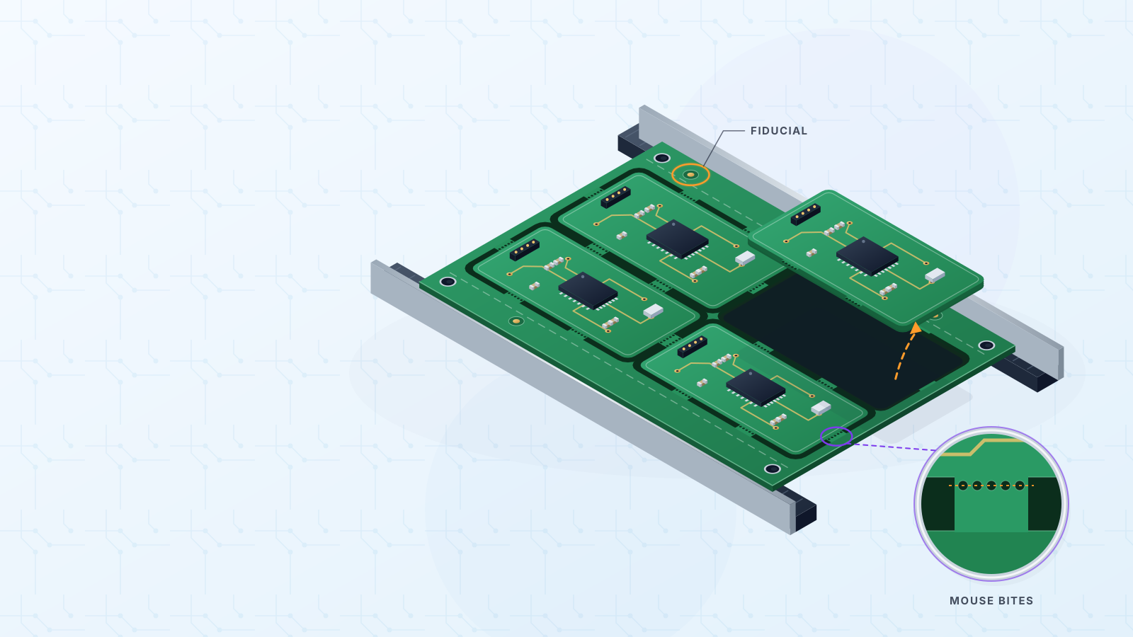
- 4Add fiducials so the printer and placer can align themselves.
For the deeper version, read our solder paste, stencils and reflow guide, see the stencil types on stencil solutions, and use design for assembly for layout rules. Then upload your files for an instant assembly price.
#solder-paste#smt-stencil#reflow-profile#smt-defects#pcb-assembly
Get an instant PCB quote