From Gerber to Doorstep: The Journey of Your PCB
Follow one PCB order from Gerber upload through engineering check, fabrication, free 100% electrical test and express delivery — and learn what you can do at each step to keep it moving.
Microplacer team · 15 November 2026 · 5 min read
 PCB Manufacturing
It is late on a Thursday. Priya, a hardware engineer in Pune, has just finished routing a four-layer sensor board and exported her Gerbers. She zips the folder, clicks upload, and goes to bed. What happens to that zip file between her click and the courier ringing her doorbell? Let us follow her order, step by step.
Step 1: The upload — the board measures itself
As soon as the archive finishes uploading, the quote page parses her Gerbers and works out the board dimensions on its own, using the outline layer. She does not have to type a width or height — but she does have to glance at the result.
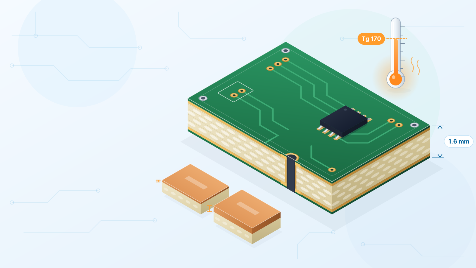
Automatic does not mean blind, though. Priya checks the size against her CAD tool, because a missing or doubled outline can make a board look bigger or smaller than it is. She then picks her options — four layers, 1.6 mm, green mask, ENIG, ten boards — and the price updates as she goes. FR-4 and flex boards up to 16 layers get an instant price, and the online price already includes GST and shipping. The minimum is 5 PCBs per design, so ten is no problem.
She saves the quotation and places the order the next morning, paying at order time by online payment. A bank transfer works just as well.
Step 2: A real engineer opens the files
Before any copper is touched, our engineers check the files. A human review is the cheapest place to catch slips such as an absent drill file, a design with more layers than the quote, clearances below what the process can hold, or a logo that landed on a copper layer instead of the silkscreen.
Priya had added a small README in her zip saying "Impedance-sensitive USB pair, please keep stack-up standard". Production notes like this are read and compared with the options she chose. If a note and the order disagree, that is raised as a question rather than guessed at — which is exactly why it pays to write notes clearly and to answer quickly.
Step 3: Building the board, layer by layer
Once the files are cleared, CAM engineers turn them into production tooling and place copies of the board on a large working panel. Then the physical work starts. Simplified, a four-layer build like Priya's runs in this order:
- 1Inner layers. The core that will become layers 2 and 3 gets a photosensitive resist, is exposed to her pattern, and the unprotected copper is dissolved away. The result is checked before anything is hidden inside the stack.
- 2Lamination. That core is sandwiched between sheets of resin-filled glass cloth (prepreg) and thin copper foil, and a hot press bonds the whole sandwich into a single rigid panel.
- 3Drilling. Holes for vias and through-hole leads are drilled. At this point the holes are just bare glass and resin.
- 4Plating. A thin conductive seed layer is laid on the hole walls so copper can then be electroplated over it — this copper tube is what links one layer to the next.
- 5Outer layers. Layers 1 and 4 now get her top and bottom pattern: the track image is printed, built up with plating, and the leftover copper is etched off.
A one- or two-layer board skips the first two steps.
Step 4: Solder mask, silkscreen and surface finish
Next come three finishing layers, each with a clear job:
| Stage | What it does | What to check in your design |
|---|---|---|
| Solder mask | A coloured polymer layer over the tracks that leaves only the pads exposed, so solder stays where it belongs. | Every pad you plan to solder has a mask opening; the colour itself does not change performance. |
| Silkscreen | The ink legend: part references, polarity marks, outlines and your logo. | Keep text off pads and readable — tiny text can blur. |
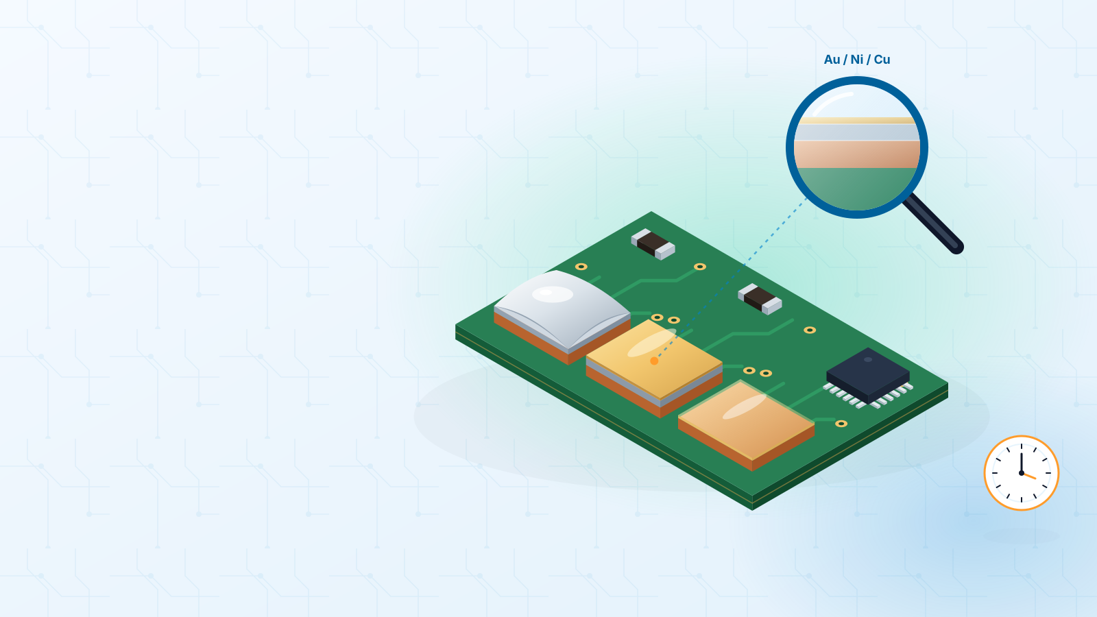
| Surface finish | A coating on the exposed copper that keeps it solderable until assembly. | ENIG gives flat pads for fine-pitch parts; HASL suits simple boards. |
Priya chose ENIG because her board carries a fine-pitch QFN, and a flat pad surface makes paste printing and soldering more predictable.
Step 5: Every board gets tested, for free
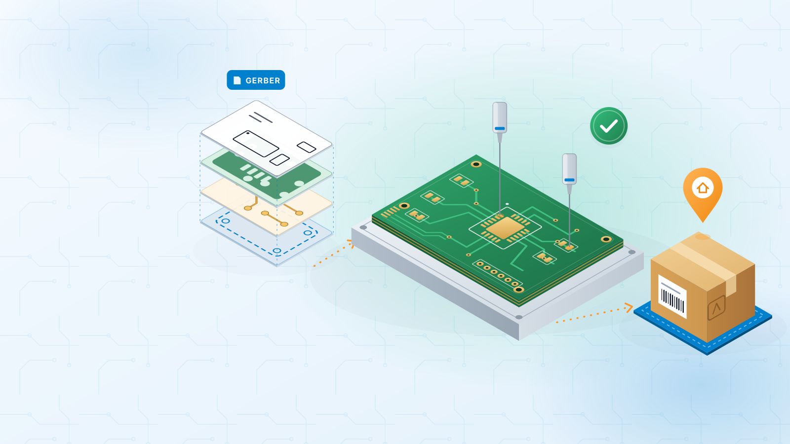
Before the boards are cut out of the panel and shipped, each one goes through a flying-probe electrical test. Moving probes touch the net points and compare the real board against the design data, catching opens (a broken connection) and shorts (two nets touching that should not).
- 100% of boards are tested — not a sample from the batch.
- There is no extra charge for it; it is part of every order.
- It checks the bare board connections, not your components or firmware — that comes after assembly.
After testing, each board is cut free along its outline (or scored, if it ships as a panel), and the batch gets a last look for appearance and dimensions.
Step 6: Packing and the ride home
The finished boards are packed and handed over for express shipping. For bare PCBs, delivery is typically 10–15 working days from order, and that window already includes express shipping within India — so there is no separate courier step for Priya to arrange.
What can slow the journey down
- Files that need a question answered — reply quickly and production can continue.
- An outline or drill file missing from the zip.
- Options in the quote that do not match the design (for example, two layers chosen for a four-layer design).
Your next step
Within that window, Priya opens a box of tested boards and gets to the fun part. For the same smooth trip, read our PCB manufacturing process guide for the full step list, check the PCB manufacturing FAQ for limits and lead times, and make sure your zip is complete with the Gerber file checklist before you upload.
#pcb-manufacturing#gerber-files#flying-probe-test#lead-time#surface-finish
Get an instant PCB quote