Heavy Copper PCBs: 5 Myths About Current, Heat and Trace Width
Thicker copper, trace width calculators and thermal vias are often misunderstood. Five myths about high-current PCBs, and what really keeps power boards cool.
Microplacer team · 15 November 2026 · 5 min read
 PCB Manufacturing
Your motor driver works on the bench, then the input connector turns brown after an hour inside the enclosure. The usual reaction is "order thicker copper next time". Sometimes that is the fix, but much of what is said about heavy copper and heat is half true. Here are five myths, and what actually happens.
Myth 1: Thicker copper is always better
Going from 1 oz (about 35 µm) to 2 oz (about 70 µm) doubles the copper in every trace, so the same track runs cooler and loses less voltage. Nobody disputes that. What the myth leaves out is the bill: gaps must open up, fine-pitch parts get harder to route, and the board uses more copper and more process time.
Plenty of power boards carry several amps on 1 oz or 2 oz copper because the layout does the work — wide pours, the same net on both layers stitched together, short paths. Use heavy copper when space is truly tight, not by default.
Myth 2: A trace width calculator settles everything
No trace comes with a built-in amp rating. Every trace turns some current into heat (I²R), and "wide enough" simply means the trace stays within a temperature rise you have decided you can live with — 10 °C is a popular, cautious target. A calculator does that arithmetic for you, but only for the inputs you give it.
- Which standard is behind it? Plenty of online tools still draw on the legacy IPC-2221 curves. IPC-2152 replaced them with measured data that factors in board thickness and nearby planes, and it can give a noticeably different width.
- Which current did you enter? Feed it the worst-case RMS value, then add headroom for start-up surges and sustained peaks — the average flatters you.
- What about voltage drop? On a 3.3 V or 5 V rail, a long trace can stay cool and still lose more millivolts than the load tolerates. And warm copper resists more — around 0.4% extra per degree — so the drop grows as the board heats up.
- Where are the necks? The maths assumes one constant width. In a real layout the current has to pass every pinch point — a gap between two pads, a single connector pin — and the hottest spot is wherever the copper is thinnest.
Myth 3: Heat only leaves through the copper on top
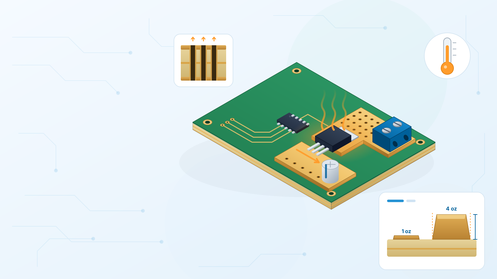
Copper moves heat over a thousand times more easily than glass-epoxy, so it is tempting to picture the top layer doing all the work. In fact heat runs along copper in every layer, hops between layers through plated holes, and escapes from both faces into the air, the case and the mounting hardware.
That is why an outer trace usually handles more current than an inner one of the same size: the inner trace is wrapped in laminate and must push its heat through it first. It is also why a solid inner ground plane under a hot part, joined by vias, is an excellent hidden heat spreader. And it explains the brown connector from the opening: in a closed enclosure the trapped air warms up, so every part starts hotter.
Myth 4: Thermal vias are optional decoration
FR-4 is close to an insulator through its thickness, so without vias the heat from an exposed pad on a QFN, D-PAK or LED has almost nowhere to go. One plated hole conducts very little heat, but a grid of them acts in parallel and cuts the thermal resistance sharply. Current behaves the same way. The copper in a via is the thin plating on its wall, which does not get thicker when you order heavier layers — so a lone via between two 2 oz pours can be the hottest point on the whole path.
| Situation | Common starting point (general guidance) |
|---|---|
| Exposed pad under a QFN or power part | Follow the datasheet land pattern first; otherwise an even grid of small (roughly 0.2–0.35 mm) vias about 1 mm apart |
| Where the vias land | A real copper pour or plane on the other side, at least as large as the pad |
| Moving several amps between layers | Several vias in parallel, spread across the full width of the pour |
| Solder wicking down in-pad vias | Have them filled and capped, or use small vias covered with mask on the opposite side |
Myth 5: Heavy copper does not affect fine features or cost
Etching chemistry cannot tell down from sideways. While it works through a thick layer, it also nibbles under the edges of the resist, so heavy-copper tracks finish narrower on top than at the base and need bigger gaps between them. Fine-pitch pads and skinny traces between pads are hit first. Tall copper also leaves deeper valleys for prepreg resin to fill in lamination and taller edges for solder mask to cover.
So it costs more for physical reasons: extra metal and longer plating, etching and pressing. Assembly feels it too — big copper areas pull heat from the joint, so give soldered pads on large pours thermal-relief spokes.
Practical takeaways for high-current layouts
- 1Decide copper weight before routing, from the worst-case current and an allowed temperature rise.
- 2Use pours rather than traces for several amps, and run the net on both layers with via stitching.
- 3Check every neck: pads, connector pins and single vias between layers.
- 4Put a via grid under every exposed thermal pad, landing on real copper.
- 5Write high-current nets and copper weight per layer in your fabrication notes — our engineers read them during the file check.
- 6Build a small prototype batch and measure temperatures at full load, inside the real enclosure.
Ready to go deeper? The heavy copper and high-current PCB guide has width tables, via current estimates and ordering tips, and the PCB thermal management guide covers thermal vias and placement. When your layout is ready, upload your Gerber for an instant price including GST and shipping.
#heavy-copper#high-current#trace-width#thermal-management#thermal-vias
Get an instant PCB quote